This simple circuit allows you to create a flashing indicator that you can use for a variety of purposes. For example, you can pretend that your car has an alarm system fitted by mounting this inside the dash, and having a blinking red LED visible from outside the car.
Because the circuit is easy to assemble, this is a great first project if you are just learning how to solder and to assemble printed circuit boards. Making an LED blink is a rite of passage for anyone who works with electronics!
Parts required
Resistors:
- R1: 330 ohms (orange-orange-brown-gold)
- R2: 47K ohms (yellow-violet-orange-gold)
- R3: 47K ohms (yellow-violet-orange-gold)
- R4: 330 ohms (orange-orange-brown-gold)
Capacitors:
- C1: 2.2uF 16V electrolytic
- C2: 10uF 16V electrolytic
Semiconductors:
- LED1: Red light emitting diode
- LED2: Green light emitting diode
- Q1: NPN transistor 2N2222 or similar, such as BC548
- Q2: NPN transistor 2N2222 or similar, such as BC548
Miscellaneous:
- 9V battery (note: not included in the kit due to postage restrictions)
- 9V battery connector
- Printed circuit board
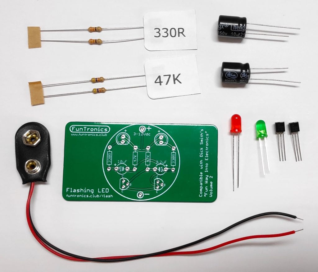
A complete kit with all the parts spread out:
Assembly
There are many tips and tricks in the PCB Assembly Tips section. Make sure you read them before beginning assembly, and also read the Learning To Solder section if you haven’t soldered before.
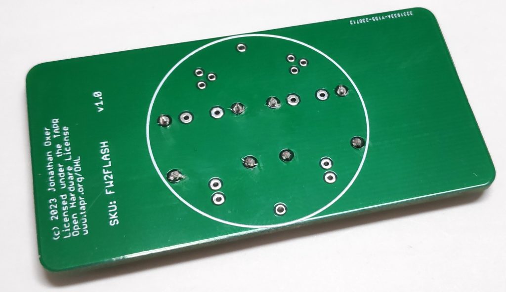
Step 1: Check the parts and identify them
If you have bought a FunTronics kit, everything should be included except the battery. You will need to provide your own 9V battery.
The photo above shows all the parts. Make sure you can identify what each part is before you continue, and make sure nothing is missing. If you can’t tell the resistors apart, you can use a multimeter to measure their values.
Step 2: Resistors
There are four resistors in the circuit. There are two different values used, so make sure you know which one goes in each location. The PCB has the values printed on it. Use either a small pair of pliers or a 3D-printed lead bending jig to bend the leads at right angles, so that they can be inserted easily into the PCB:
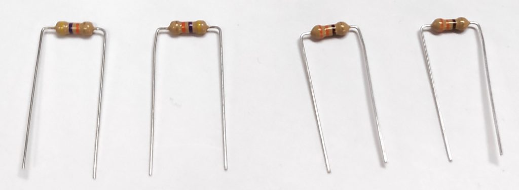
Resistors are not polarised, so you can insert them either way and they will work just fine. However, it’s standard practice to align resistors so that their colour codes all read in the same direction for convenience later if you need to read them, but it doesn’t make any difference to their operation.
The usual convention is to read the colours from left to right, or top to bottom, depending on the orientation of the part. In this case the resistors are aligned vertically, so the last stripe (gold) goes towards the bottom.
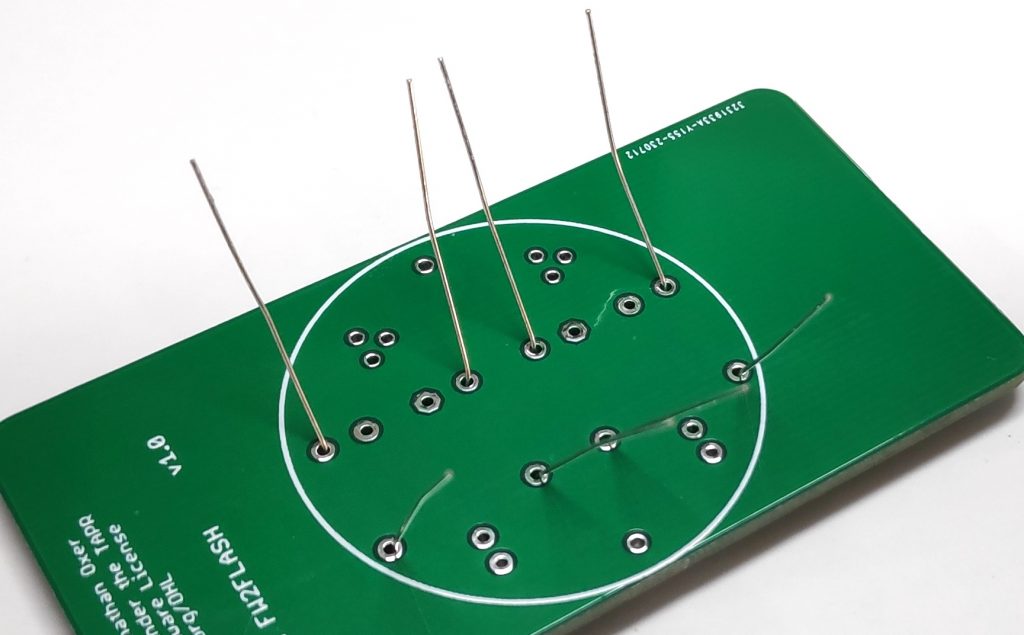
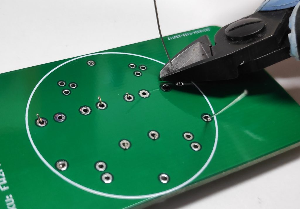
Then bend the leads out to hold the resistors in place, and cut them off about 2mm from the surface of the PCB before soldering them in place:
 |  |  |
Step 3: LEDs
Unlike resistors, Light Emitting Diodes are polarised. That means it’s critical which way around you install them. Through-hole LEDs typically have a flat spot on the side of the case, and one leg longer than the other. The longer lead goes to the “+” side on the PCB.
There is also a flat orientation marker that you can find on the body of the LED, which is on the cathode (negative) side which is towards the bottom of the PCB.
Insert the LEDs and bend their leads out to hold them in place. Cut the leads off below the PCB and solder them in place, just like the resistors:
PIC
Step 4: Capacitors
Some types of capacitors are polarised, and some aren’t. These particular capacitors are polarised, so you have to be careful which way you insert them. The longer lead goes to the “+” side on the PCB, and you will also find a marking on the body of the cap that shows you which is the negative “-” pin.
You know the drill by now: insert, bend, clip, solder!
Step 5: Transistors
We’ve left these to last because they’re the trickiest of the parts in this project. Not only do they have three leads, but the connections are close together on the PCB so you need to be careful when soldering them.
Gently bend the leads so that they can be inserted into the offset holes in the PCB. The outer pins go in a line, and the middle pin is offset to one side.
Note: DO NOT push the transistors down hard against the PCB! They are designed to sit up away from the board so that their leads are not deformed too sharply, as shown in the photo.
Insert them so that the PCB is about half way along the leads, then bend them out to hold them in place before trimming and soldering.
Step 6: Battery connector
The battery connector has red and black wires. Insert the red wire into the “+” pad on the PCB, and the black wire into the “-” pad.
The wires should be inserted so that the plastic insulation is pushed up against the PCB. Solder them in place, and trim off the excess lead.
Step 7: Check you work!
Stop! I know you want to plug it in right away, but take a moment to look at the position of the parts on the board. Also look carefully at the solder joints on the bottom of the PCB to make sure there are no solder bridges between any of the pads. In particular, look at the pads for the transistors because they’re close together. If there’s a solder bridge on the board, that’s probably where it’ll be.
If there are any problems, fix them before going any further. See the handy Rework Techniques page for information on ways to do things like remove parts from the board if you’ve put them in the wrong place.
Step 8: Connect power
Connect your 9V battery to the battery connector. The pair of LEDs should immediately begin flashing exactly out of time: when one LED is on, the other is off.
What if it doesn’t work?
check battery
visual inspection
How it works
At first glance this circuit doesn’t make much sense. It’s strangely symmetrical but how it works isn’t immediately obvious. It’s a very clever circuit that uses only a few parts to create a useful electronic building block that can be used in larger, more complex projects.
You’ll notice that the layout of the schematic and the physical PCB are very similar. This was done deliberately for this project so that when you are looking at the PCB, it’s easy to see how the schematic matches up to it. On most circuits this is not the case, and it takes more work to match up the parts in the schematic to the parts on the board. However, when you’re just getting started this is a good way to see how the virtual and physical representations of the circuit correspond:
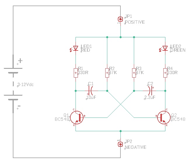
Technically this circuit is called an astable multivibrator: “astable” because it’s not stable in any state and keeps flipping between its possible states all by itself, and “multivibrator” because it produces two square waves that are exactly out of synchronisation. When one is high, the other is low and vice versa. In this project we use those square waves to turn on LEDs, so they blink on and off exactly out of phase.
Starting with just the left side of the circuit, have a look at the path formed by LED1, R1, and Q1. If transistor Q1 is turned on, current could flow from the positive terminal at the top down through LED1, then through R1, then into the Collector pin of Q1 and out of its Emitter pin all the way to the negative terminal. The LED would then turn on, with the current being limited by R1 to prevent the LED from burning out.
Likewise, the right side of the circuit forms a direct path from the positive terminal through LED2, then R4, and then Q2 all the way to the negative terminal. If transistor Q2 is turned on, LED2 will illuminate.
So the big question is: how do Q1 and Q2 get turned on so that their LEDs can illuminate?
Transistors Q1 and Q2 are controlled via their Base pins. When the voltage applied to the Base is high, they turn on and allow current to flow from the Collector to the Emitter. When the voltage applied to the Base is low, they turn off and prevent current flowing.
When power is first applied to the circuit, the positive side of C1 will begin charging up via LED1 and R1, and the positive side of C2 will begin charging up via LED2 and R4.
However, the voltage of the negative side of both capacitors will also begin to rise as they are charged up via their 47K resistors!
Therefore the voltage on both sides of the capacitors rises, but the voltage on their positive terminals will rise much faster than the voltage on the negative terminals due to the difference in resistance.
But what effect does this rising voltage have on the rest of the circuit?
You can see in the schematic that the negative terminal of C1 is connected to the base of Q2, and the negative terminal of C2 is connected to the base of Q1. If the voltage of the negative terminal of a capacitor reaches a certain threshold, it will cause the transistor attached to it to turn on.
It’s a race! Only one capacitor can win: they won’t both reach the point of turning on their transistor at the exact same moment.
Imagine that C2 just happens to charge more quickly. That means transistor Q1 will turn on first, when the voltage on the negative terminal of C2 goes past the critical threshold. Turning on Q1 allows current to flow through LED1, R1, and Q1, so the red LED will turn on.
But that’s not all. Because Q1 has turned on, the voltage at its Collector will drop to a very low level: probably about 1V, depending on the characteristics of the transistor.
Hang on, what does this mean for C1? If C1 was charging up, and Q1 is now turned on and has pulled its Collector to 1V, what happens?
By this point there will be a voltage differential across C1 of perhaps 6V. That means if the positive terminal of C1 is pulled hard to 1V, it will force the negative terminal of C1 to go about 6V below that, so the negative terminal will go to about minus 5V!
This will have the effect of turning off transistor Q2 hard, because it’s now seeing a negative voltage at its Base.
With Q2 turned off, the negative side of C1 will begin to rise via R2.
And this is where the magic happens. At a certain point the negative side of C1 will rise high enough that it will turn on Q2. This then causes its Collector to be pulled down to about 1V, which pulls the positive side of C2 down to about 1V, which now causes the negative side of C2 to go to about minus 5V! Q1 is then forced to turn off, and the circuit has flipped into its opposite state.
The process repeats itself indefinitely: one half of the circuit stays on for a while until the other one reasserts itself and turns on, which turns off the other. The circuit flip-flops between one side being on, then the other side being on.
Lost? Don’t worry, this is a tricky circuit to understand. One day you’ll come back to it and it will start to make more sense.
What to do next
aoeu
Change flash rate